Construction workers in safety gear pose with U.S. and South Korean flags between excavators at a groundbreaking site with cranes in the background.
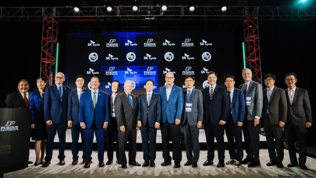
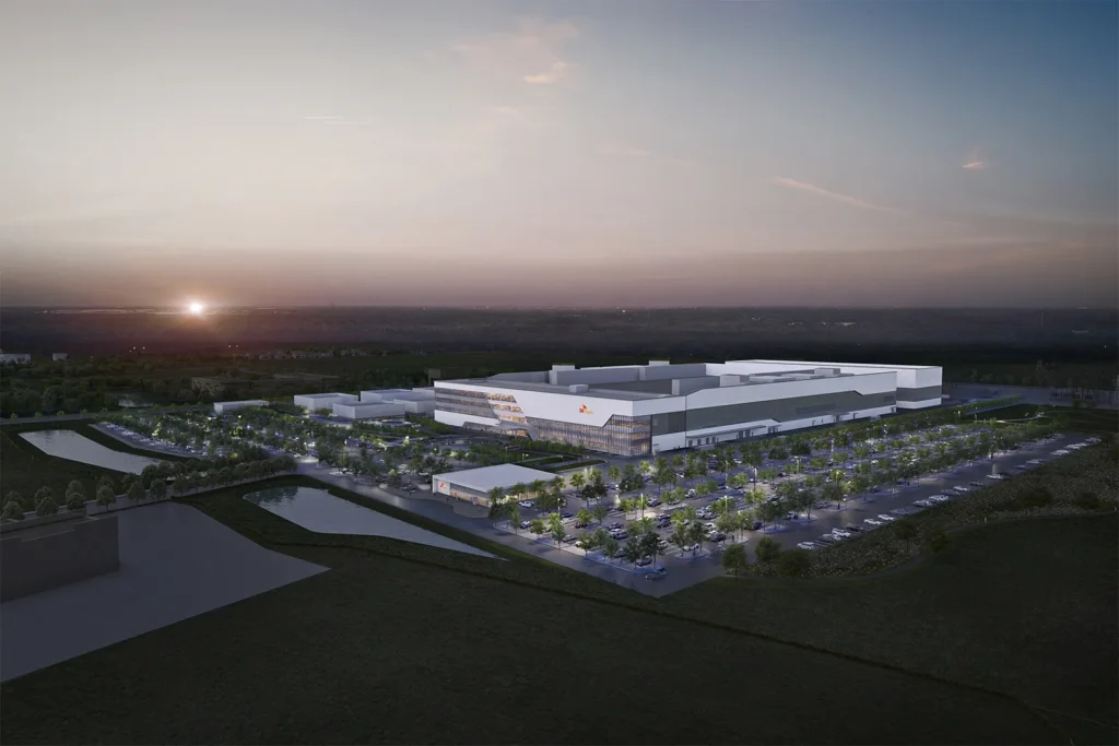
SK hynix held a groundbreaking ceremony on August 27 at Purdue University in West Lafayette, Indiana, for an advanced packaging production facility dedicated to AI memory. The event was attended by Indiana Governor Mike Braun, US Senator Todd Young, Purdue University President Mitch Daniels, and Robert Abrams, Chairman of the Korea-US Alliance Foundation, as well as SK Group Vice Chairmen Yu Jeong-Joon and Lee Hyung-hee, and SK hynix CEO Kwak Noh-Jung. South Korean Ambassador to the United States Kang Kyung-wha also attended.
| Attribute | Details |
|---|---|
| Total investment | Exceeding $4 billion |
| Cleanroom opening | October 2028 |
| Mass production start | Second half of 2029 |
| Product | Next-generation HBM |
| Commercial operations workforce | Approximately 1,000 workers |
The Indiana facility represents SK hynix's first High Bandwidth Memory (HBM) production base in the United States. With a total expected investment exceeding $4 billion, the fab is scheduled to open its cleanroom by October 2028 and begin mass production of next-generation HBM in the second half of 2029. The facility will employ approximately 1,000 workers during commercial operations.
The operation will integrate closely with SK hynix's Korean production: cutting-edge wafers produced in South Korea will be shipped to Indiana for advanced packaging and testing before being supplied to US customers as Made in USA products. An “Advanced Packaging R&D Testbed” will also be built alongside production lines, enabling customers, universities, and business partners to collaboratively develop next-generation packaging technologies and conduct prototype fabrication and performance validation.
This project will create good-paying jobs, strengthen our national and economic security, and ensure the technologies of the future are developed and manufactured here in the United States. I was proud to help make this investment possible through the CHIPS and Science Act.
“This project will create good-paying jobs, strengthen our national and economic security, and ensure the technologies of the future are developed and manufactured here in the United States,” Senator Young said. “I was proud to help make this investment possible through the CHIPS and Science Act.”
This project will usher in the next generation of American innovation, bring thousands of good-paying jobs to Indiana and supercharge regional economic development.
Governor Braun added, “This project will usher in the next generation of American innovation, bring thousands of good-paying jobs to Indiana and supercharge regional economic development.”
SK hynix expects the Indiana fab to help stabilize the US semiconductor supply chain and contribute to strengthening national security and the economy amid intensifying competition to expand AI infrastructure.
More than 100 companies are being considered as suppliers for materials, components, and equipment for the facility, supporting stable operations and solidifying the US AI ecosystem. SK hynix plans to create approximately 7,000 direct and indirect jobs with local and national companies during facility construction and subsequent commercial operations.
SK hynix's investment in Indiana is not merely an investment in semiconductor manufacturing facilities, but the establishment of the first AI memory production facility and R&D center in the United States, creating a unique model for nurturing semiconductor talent and strengthening collaboration with the government and external organizations.
Ambassador Kang noted that “SK hynix's investment in Indiana is not merely an investment in semiconductor manufacturing facilities, but the establishment of the first AI memory production facility and R&D center in the United States, creating a unique model for nurturing semiconductor talent and strengthening collaboration with the government and external organizations.”
SK hynix signed a Memorandum of Understanding with Purdue University for research and development collaboration in advanced packaging. The partnership will strengthen R&D cooperation and jointly research system integration and advanced packaging technologies, including HBM. SK hynix also plans to expand recruitment of world-class talent from across the Midwest.
The company established a recruitment partnership to honor Indiana's historical connection to the Korean War, during which the state deployed approximately 140,000 troops. SK Group agreed to provide employment and career opportunities for discharged USFK service members through participation in the ‘USFK Veterans Job Platform' operated by the Korea Chamber of Commerce and Industry and the Korea-US Alliance Foundation.
The United States is the epicenter of AI innovation, bringing together premier customers, top-tier R&D capabilities, and partners. Indiana fab will become a gateway to deliver first Made in USA HBM products. We will expand our investments and collaboration in the US, grow together, and become the most trusted partner in shaping the future of AI in America.
CEO Kwak Noh-Jung said, “The United States is the epicenter of AI innovation, bringing together premier customers, top-tier R&D capabilities, and partners. Indiana fab will become a gateway to deliver first Made in USA HBM products. We will expand our investments and collaboration in the US, grow together, and become the most trusted partner in shaping the future of AI in America.”
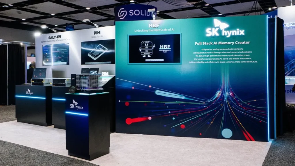
SK hynix has not published a complete specification sheet for the HBM4E products planned for its Indiana facility. The company says the plant will package and test next-generation HBM, with cleanroom operations scheduled by October 2028 and mass production planned for the second half of 2029; company executives have identified the planned product as seventh-generation HBM4E, according to Reuters. For context, SK hynix's currently disclosed HBM4 specification includes a 12-layer stack and 2,048 input/output channels—twice the previous generation—while its HBM3E portfolio includes a 36 GB product. The available sources do not provide confirmed HBM4E figures for capacity, bandwidth, layer count, interface speed, or power consumption.
| Specification | HBM3E | HBM4 | HBM4E planned for Indiana |
|---|---|---|---|
| Generation | Fifth | Sixth | Seventh |
| Announced capacity | 36 GB | Not specified | Not disclosed |
| Stack configuration | 12-layer product shown | 12 layers | Not disclosed |
| Input/output channels | Not specified | 2,048 | Not disclosed |
| Bandwidth | Not specified | Not specified | Not disclosed |
| Power efficiency | Not specified | More than 40% higher | Not disclosed |
| Indiana production timing | Not specified | Not specified | Second half of 2029 |