AMD Begins Production Ramp of Venice EPYC Processor on TSMC 2nm Technology
AMD has begun ramping production of its next-generation Venice EPYC processor on TSMC's cutting-edge 2nm process technology in Taiwan, with plans to expand manufacturing to Arizona. This marks the industry's first high-performance computing chip to reach production on such an advanced node, signaling AMD's commitment to delivering the performance and efficiency modern AI infrastructure demands.
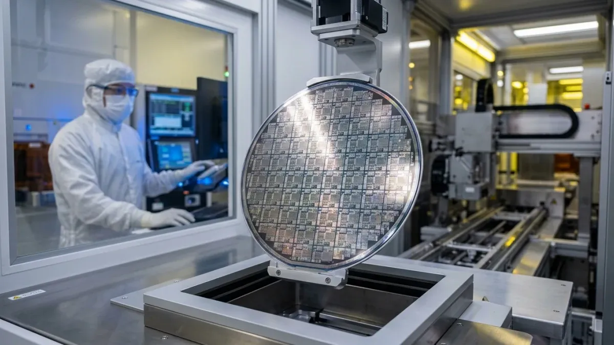
A silicon wafer with numerous processor dies sits on a machine in a cleanroom, with a technician in protective gear monitoring equipment in the background.
AMD announced that its next-generation EPYC processor, codenamed “Venice,” is ramping production in Taiwan on TSMC's advanced 2nm process technology, with future plans to ramp production at TSMC's Arizona fabrication facility. “Venice” is the first high-performance computing product in the industry to enter production on TSMC's 2nm process.
The milestone reflects AMD's execution of its data center CPU roadmap and demonstrates progress toward delivering leadership performance and energy efficiency for next-generation cloud, enterprise, and AI infrastructure.
Ramping ‘Venice' on TSMC 2nm process technology marks an important step forward in accelerating the next generation of AI infrastructure. As AI and agentic workloads scale rapidly, customers need platforms that can move from innovation to production faster. Our deep partnership with TSMC is helping AMD bring leadership compute technologies to market with the speed and scale required to meet this moment.
As AI adoption expands from training and inference to increasingly complex agentic workloads, the CPU is becoming more critical to scaling AI infrastructure. It coordinates data movement, networking, storage, security, and system orchestration across the data center. The ramp of “Venice” reflects growing customer demand for EPYC processors to power modern cloud, enterprise, HPC, and AI deployments.
The “Venice” ramp in Taiwan and plans to ramp at TSMC Arizona reflect AMD's focus on strengthening its geographically diverse advanced manufacturing footprint. By pairing next-generation EPYC processor innovation with advanced manufacturing capacity globally, AMD is expanding the foundation needed to support customers deploying and scaling AI infrastructure.
We are pleased to see AMD continue to make strong progress with its next-generation EPYC processor on our advanced 2nm process technology. Our close collaboration with AMD reflects the importance of pairing leadership process technology with advanced design innovation to enable the next era of high-performance and AI computing.
AMD also plans to extend TSMC 2nm process technology across its data center CPU roadmap with “Verano,” a 6th Gen EPYC processor optimized for performance-per-dollar-per-watt leadership. Designed for cloud and AI computing workloads, “Verano” is expected to build on the AMD EPYC platform with advanced memory innovations, including LPDDR, to deliver the CPU performance, bandwidth, and efficiency required for increasingly power-constrained workloads and applications.
AMD and TSMC's partnership spans technologies needed to scale modern data center computing, from TSMC 2nm process technology for next-generation CPUs to advanced packaging technologies, including TSMC's SoIC-X and CoWoS-L, used across AMD's broader AI and data center portfolio. With “Venice” ramping on TSMC 2nm, AMD is advancing the CPU foundation for AI infrastructure while continuing to leverage TSMC's process and packaging leadership to deliver increasingly integrated compute platforms at scale.