SK Hynix Invests 54 Trillion Won in New Yongin and Cheongju Fabs
SK Hynix is betting big on artificial intelligence. The South Korean chipmaker just greenlit a colossal 54 trillion won investment to build next-generation memory factories in Yongin and Cheongju, signaling confidence that AI demand for chips isn't a fleeting spike—it's structural change reshaping the entire industry.
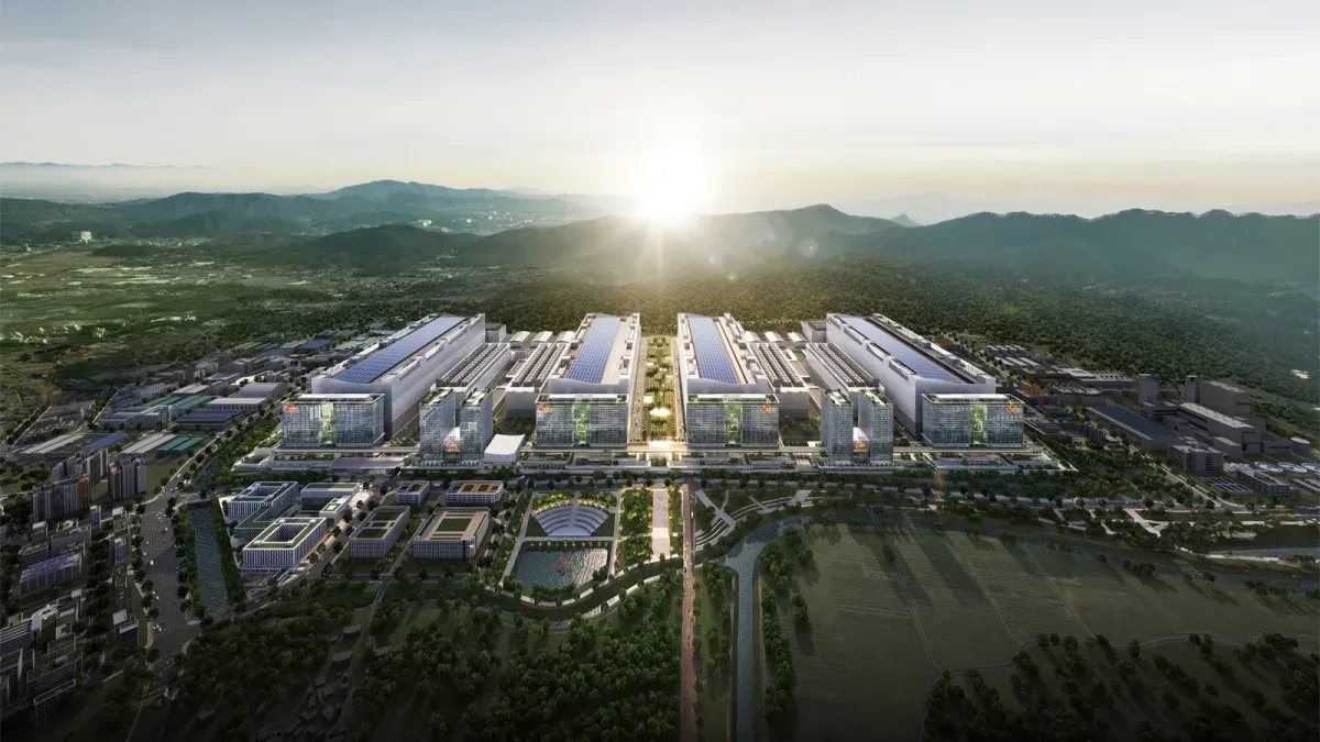
Aerial view of a modern industrial complex with large white buildings, green landscaping, and mountains in the background at sunrise.
SK hynix Inc. announced that it has approved a total investment of approximately 54 trillion won to build new fabs in Yongin and Cheongju to meet growing demand for memory in the AI era. The company will invest 35.2 trillion won in the Yongin “Y2” fab and 19.1 trillion won in the Cheongju “M17” fab, according to a board decision.
Facility
Investment
Yongin Y2 fab
35.2 trillion won
Cheongju M17 fab
19.1 trillion won
Total
54 trillion won
This investment executes the mid-to-long-term strategy the company announced last June. SK hynix is currently constructing its first fab in Yongin (Y1) under a master plan to invest 600 trillion won in the Yongin Semiconductor Cluster and 100 trillion won to expand its Cheongju production base. With this latest decision, the company is embarking on construction of subsequent fabs in both locations.
According to market research firm Omdia, both DRAM and NAND demand are projected to maintain a compound annual growth rate (CAGR) of 19% from 2025 through 2030. SK hynix views this growth not as a temporary supercycle, but as structural transformation in which memory becomes core infrastructure determining AI performance itself.
An SK hynix official stated: “This investment is a decision made to seize opportunities in line with the market's growth speed. By proactively securing production capabilities, we aim to establish ourselves as a key partner in AI infrastructure, contributing to the stability of the global AI semiconductor supply chain.”
This investment is a decision made to seize opportunities in line with the market's growth speed. By proactively securing production capabilities, we aim to establish ourselves as a key partner in AI infrastructure, contributing to the stability of the global AI semiconductor supply chain.
Yongin Y2 Facility
Yongin Y2 will serve as a DRAM production base spanning 341,000 pyeong (approximately 1,130,000m²). Construction is scheduled to break ground in July 2027, targeting the opening of its first cleanroom in June 2029 to produce high-bandwidth memory (HBM) and other next-generation DRAM products. Construction on the Y1 fab is progressing smoothly toward its initial cleanroom opening target of February 2027.
Specification
Details
Size
341,000 pyeong (approximately 1,130,000m²)
Groundbreaking
July 2027
First cleanroom opening
June 2029
Production focus
High-bandwidth memory (HBM) and next-generation DRAM
Investment period
Through October 2031
SK hynix previously set a goal to accelerate the Yongin Semiconductor Cluster completion by 12 years—from the originally planned 2045 to 2033—to finish constructing all four fabs. The Y2 construction serves as the second phase supporting this accelerated timeline, with investments spanning to October 2031.
The investment amount includes construction costs for a Business Support Building with administrative and welfare facilities for Y2 personnel, an Integrated R&D Center to consolidate product development testing, analysis, and experiments, and auxiliary infrastructure.
The Yongin Semiconductor Cluster sprawls over approximately 1.26 million pyeong (approximately 4,160,000m²) in Wonsam-myeon, Cheoin-gu, Yongin-si, Gyeonggi-do. Phase 1 power and water infrastructure required through Y2 operation is nearing completion at a 99% progress rate. With fab construction and infrastructure setup carried out concurrently, the company plans to proceed with Y2 construction on schedule.
Cheongju M17 Facility
In the NAND market, demand is surging rapidly, driven by enterprise SSDs as AI services expand at scale. This is further boosted by demand for key-value (KV) cache storage in AI inference, with application fields expected to broaden as agentic and physical AI are introduced.
SK hynix selected Cheongju as its new NAND fab base because it offers the fastest fab construction timeline. The Cheongju Campus already houses the M11, M12, and M15 fabs, enabling efficient production linked to existing operations on sites with substantial pre-established power and water infrastructure. Cheongju M17 will span 206,000 pyeong (approximately 680,000m²), breaking ground in February 2027 with plans to open its first cleanroom in December 2028. The investment period runs through April 2031.
Specification
Details
Size
206,000 pyeong (approximately 680,000m²)
Groundbreaking
February 2027
First cleanroom opening
December 2028
Investment period
Through April 2031
Production and Capital Strategy
SK hynix plans to proactively secure production infrastructure based on mid-to-long-term demand discussed with customers, while expanding actual production capacity in alignment with customer needs. Fabs will be constructed according to the master schedule, whereas cleanroom expansions and equipment installation will take place sequentially in line with demand trends to maximize capital efficiency.
The company expects this investment to secure future growth foundations while strengthening the competitiveness of the domestic semiconductor ecosystem and boosting local economies. The simultaneous investments in Yongin and Cheongju are anticipated to expand joint growth opportunities for supply chain partners, generate employment, and revitalize local commercial districts.